Transistors are fundamental components in analogue electronics, enabling amplification, switching, and signal modulation. In the Kenyan electrical engineering sector, knowledge of transistors is essential for designing and maintaining equipment ranging from communication systems to control circuits in manufacturing plants. This chapter focuses on the bipolar junction transistor (BJT), a widely used transistor type in power amplifiers, signal processing, and control devices. Understanding the types, construction, operation, and characteristics of BJTs equips engineers with the skills to apply these devices effectively in practical scenarios such as instrumentation panels at county government offices or automated systems in Kenyan textile factories.
3.1 Bipolar Junction Transistors (BJTs)
BJTs are semiconductor devices that use both electron and hole charge carriers for operation, making them versatile for amplification and switching in analogue circuits. Their performance characteristics and operational principles are critical for electrical engineers working on analogue systems in Kenya’s industrial and infrastructure projects. Mastery of BJT types, construction, and behavior under different electrical conditions enables precise control and optimisation of circuit performance.
3.1.1 Types and Construction of BJT Transistors
The BJT transistor comes primarily in two types, distinguished by their doping arrangement and charge carrier movement. These types influence how the transistor is integrated into circuits for amplification or switching in various electrical engineering applications.
Types of BJTs
- NPN Transistor: Consists of two n-type semiconductor layers separated by a p-type layer. Electrons are the majority charge carriers, flowing from the emitter to the collector. NPN transistors are preferred in most Kenyan industrial control systems due to their higher electron mobility, which allows faster switching speeds.
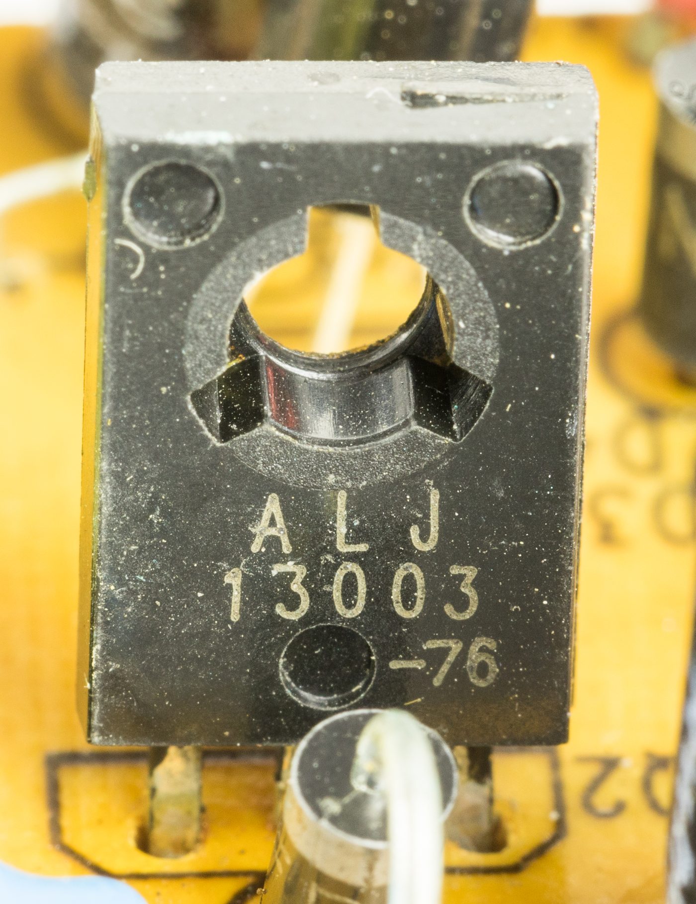
NPN transistor on circuit board (Source: Wikimedia Commons)
- PNP Transistor: Comprises two p-type layers separated by an n-type layer. Holes are the majority charge carriers, moving from the emitter to the collector. PNP transistors are often used in complementary circuits where negative voltage operation is required, such as in audio amplifier stages for hotel sound systems.
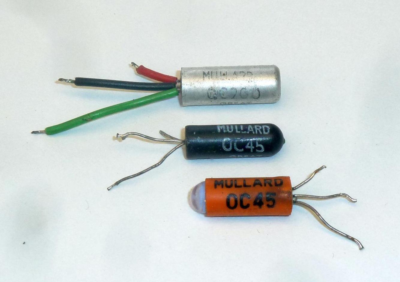
Three physical pnp transistors (Source: Wikimedia Commons)
- Complementary Pairs: NPN and PNP transistors are often paired to form push-pull amplifier configurations, common in power amplifiers within broadcast and communication equipment at universities.
- Small Signal vs Power BJTs: Small signal BJTs handle low currents and voltages, suitable for signal amplification in measurement devices at hospitals. Power BJTs manage higher currents and voltages, ideal for driving motors or lighting systems in agricultural irrigation projects.
- Discrete vs Integrated BJTs: Discrete BJTs are standalone devices used in repair and prototyping, while integrated BJTs are embedded in ICs, such as operational amplifiers in industrial automation systems.
Construction of BJTs
- Emitter: Heavily doped to inject majority carriers efficiently into the base region. The emitter’s doping level significantly affects the transistor’s gain and switching speed.
- Base: Thin and lightly doped to allow easy passage of carriers between emitter and collector. The base thickness is critical for transistor operation, controlling the recombination rate of carriers.
- Collector: Moderately doped and larger in size to collect carriers from the base. It dissipates heat generated during operation, an important consideration in power transistors used in energy distribution systems.
- Junctions: Two pn junctions exist, emitter-base and base-collector, their biasing determines the transistor’s mode of operation.
- Encapsulation: Transistors are housed in packages such as TO-92 or TO-220, providing mechanical protection and heat dissipation. Proper packaging is essential for reliability in harsh environments like Kenyan manufacturing plants.
3.1.2 Operation of NPN and PNP Transistors
Understanding how NPN and PNP transistors operate under various biasing conditions is crucial for designing reliable circuits that respond predictably to input signals. Their complementary nature allows engineers to implement versatile circuit topologies.
Operation of NPN Transistors
- Forward-Active Mode: The base-emitter junction is forward biased, and the base-collector junction is reverse biased, enabling current amplification. This mode is widely used in signal amplification circuits in telecommunication base stations.
- Cutoff Mode: Both junctions are reverse biased; the transistor is off, allowing zero collector current. This mode is essential for switching applications like relay drivers in county government electrical systems.
- Saturation Mode: Both junctions are forward biased; the transistor acts as a closed switch with maximum collector current. This state is exploited in power switching devices such as motor controllers in Kenyan factories.
- Reverse-Active Mode: The base-collector junction is forward biased, and the base-emitter is reverse biased; seldom used but relevant in special switching circuits.
- Charge Carrier Movement: Electrons injected from the emitter into the base diffuse across the thin base and are collected by the collector, with minimal recombination.
Operation of PNP Transistors
- Forward-Active Mode: The base-emitter junction is forward biased, and the base-collector junction is reverse biased, with holes as majority carriers moving from emitter to collector.
- Cutoff Mode: Both junctions are reverse biased; no current flows, equivalent to an open switch in control circuits.
- Saturation Mode: Both junctions forward biased; transistor fully on, allowing maximum collector current flow, useful in complementary push-pull stages in audio amplifiers.
- Reverse-Active Mode: Rarely used, with reversed junction biases.
- Current Directions: Conventional current flows from emitter to collector, opposite to electron flow in NPN transistors.
3.1.3 Characteristics of BJTs: V-I and Gain
The electrical characteristics of BJTs define how they respond to voltage and current inputs, influencing circuit design and performance. Kenyan engineers must interpret these characteristics to optimise analogue circuit functionality in diverse environments.
V-I Characteristics of BJTs
The voltage-current relationship in BJTs is nonlinear and depends on the transistor’s region of operation. Understanding these curves aids in predicting transistor behaviour under varying load conditions.
- Input Characteristics: Show the base current (IB) versus base-emitter voltage (VBE) at constant collector-emitter voltage (VCE). The threshold voltage (around 0.7 V for silicon BJTs) must be exceeded for conduction, a key design parameter in sensor interface circuits.
- Output Characteristics: Illustrate collector current (IC) versus collector-emitter voltage (VCE) for different base currents. The flat region indicates the transistor’s active mode where IC is controlled by IB.
- Saturation Region: Characterised by low VCE and high IC; transistor acts like a closed switch.
- Cutoff Region: IC is nearly zero; transistor is off.
- Breakdown Region: Excessive VCE leads to avalanche breakdown; engineers must ensure operating voltages remain below this to avoid device failure.
Gain of BJTs
Gain measures the transistor’s ability to amplify current and is critical for designing amplifiers and signal processing circuits.
- Current Gain (β or hFE): Ratio of collector current (IC) to base current (IB). A typical β ranges from 20 to 300, depending on the transistor type and manufacturing process. High β values reduce base drive requirements in switching circuits.
- Voltage Gain: Depends on circuit configuration and load; in a common-emitter amplifier, voltage gain can be significant for signal amplification in communication devices.
- Frequency Response: Gain decreases at higher frequencies due to internal capacitances, influencing the design of high-frequency amplifiers used in radar systems at Kenyan airports.
- Temperature Dependence: Gain varies with temperature; engineers must consider thermal stability in power electronics for renewable energy systems.
- Gain Bandwidth Product (fT): The frequency at which current gain drops to unity; important for selecting transistors in RF applications.
Practice Questions
- Explain the structural differences between NPN and PNP transistors and their impact on charge carrier movement. (10 marks)
- Describe the operation modes of an NPN transistor and explain how each mode is utilized in electrical circuits. (12 marks)
- Using the V-I characteristics, explain how a BJT behaves in the active region and why this is important for amplification. (8 marks)
- Calculate the collector current for a BJT with a base current of 50 µA and a current gain of 150. (5 marks)
- Discuss the importance of gain bandwidth product in selecting a BJT for high-frequency applications. (5 marks)
The rest of this chapter
🔒Create a free account to open more of this chapter.
Free: practical guides, quick cards, workplace scenarios and more.
Create a free account 🔒3.2 BJT Configurations
In electrical engineering practice across Kenya, particularly in designing analogue circuits for power supplies, signal amplification, and switching applications, understanding the bipolar junction transistor (BJT) configurations is critical. BJTs are fundamen…
🔒3.3 Characteristics of BJT Connections
In Electrical Engineering practice in Kenya, understanding the characteristics of Bipolar Junction Transistor (BJT) connections is critical for designing and troubleshooting analogue circuits such as amplifiers and switches. BJTs are widely used in control sys…
🔒3.4 BJT Transistor Load Line Analysis
Load line analysis is a fundamental technique used by electrical engineers in Kenya to understand the operating limits and behaviour of BJTs in circuits. It enables professionals working in sectors such as telecommunications and manufacturing to design stable…
🔒3.5 BJT Transistor Biasing Methods
In electrical engineering practice within Kenya, particularly in the design and maintenance of analogue circuits in industrial and communication equipment, proper biasing of Bipolar Junction Transistors (BJTs) is critical. Biasing establishes the correct opera…
🔒3.6 Field Effect Transistors (FETs) - JFET & MOSFET
Field Effect Transistors (FETs) are crucial components in modern analogue and digital electronics, widely used in Kenya’s telecommunication devices, power electronics, and instrumentation. Their high input impedance and low noise characteristics make them suit…
🔒3.7 P and N channels of FETs
Field Effect Transistors (FETs) are widely used in analogue electronics due to their high input impedance and low noise characteristics. In Kenya’s electrical engineering industry, especially in analogue signal processing and switching circuits at institutions…
🔒3.8 Operation of FETs
Understanding the operation of FETs is essential for electrical engineers working on analogue electronics projects such as signal amplification and switching control systems in Kenya’s healthcare equipment manufacturing and maintenance sector. The operation pr…
🔒3.9 Characteristics of FETs
In the Kenyan electrical engineering landscape, field-effect transistors (FETs) are crucial components in analogue circuit design, especially in applications requiring high input impedance and low noise, such as signal amplification in medical equipment at Ken…
🔒3.10 Biasing Techniques of FETs
Biasing FETs correctly is essential for ensuring stable operation and optimal performance in analogue circuits. In Kenya’s electrical engineering projects, such as designing power control units for county governments or signal processing modules for telecommun…
🔒3.11 Application of FETs
Field Effect Transistors (FETs) are essential components in analogue electronics due to their high input impedance, low noise, and efficient switching capabilities. In the Kenyan electrical engineering sector, FETs are widely utilized in signal amplification,…
Chapter Summary
This chapter explored the fundamental aspects of bipolar junction transistors, beginning with the types and construction of NPN and PNP transistors and their modes of operation. It examined the key electrical characteristics of BJTs, including their voltage-current relationships and current gain. Various BJT configurations were detailed, focusing on the common emitter, common base, and common collector arrangements and their distinctive features. The analysis of BJT transistor behavior was extended through load line concepts, distinguishing between DC and AC load lines. The chapter also covered essential biasing methods for BJTs, explaining terms related to biasing stability and describing techniques such as base resistor, emitter bias, collector feedback, and voltage divider biasing. Attention then shifted to field effect transistors, highlighting the differences between JFET and MOSFET types, their P and N channel variants, and their operational principles. Finally, the characteristics, biasing approaches, and practical applications of FETs were discussed, emphasizing their role in analogue electronic circuits.
Self-Assessment
🔒 PDFDownload this self-assessment, with answers
A. Written Assessment
- Identify the two main types of bipolar junction transistors and describe their structural differences. (3 marks)
- Explain how an NPN transistor operates when used as a switch in an electrical circuit. (3 marks)
🔒20 more in this section.
Chapter Examination Questions
🔒 PDFDownload these examination questions, with worked answers
SECTION A (40 Marks) - Answer ALL Questions
- Explain the structural difference between NPN and PNP bipolar junction transistors and how this affects their operation in a switching circuit used at KPLC. (4 marks)
- Describe the function of the base, collector, and emitter terminals in a BJT and how current flow occurs among them in an NPN transistor. (4 marks)
🔒18 more in this section.
Chapter Practical Activities
Practical 1: Identify and Construct NPN and PNP BJT Transistors
Electrical Engineering · Level 5
Analogue Electronics I
PRACTICAL ASSESSMENT
TIME: 4 HOURS
⬇ PDFCandidate Instructions (Candidate Tool)
Type: Individual
INSTRUCTIONS TO CANDIDATE:
1. You are required to perform the following task:
i. Identify and construct sample NPN (2N2222) and PNP (2N2907) transistor circuits on a breadboard demonstrating correct pin configuration and basic switching with a 9V supply.
2. You have been provided with the following resources for the practical task:
| Tools & Equipment | Materials |
|---|
| Digital Multimeter | 2N2222 NPN Transistor |
| Soldering iron | 2N2907 PNP Transistor |
| Wire cutter/stripper | 9V Battery |
| Breadboard | Battery clip connector |
| Resistor 1kΩ |
| Jumper wires |
| Solder wire |
| PPE (Safety goggles, overall) |
⬇ PDFResources Required (Cutting List)
| S/N | Item | Quantity |
|---|
| 1 | 2N2222 NPN Transistor | 1 Pc per Candidate |
| 2 | 2N2907 PNP Transistor | 1 Pc per Candidate |
| 3 | Breadboard | 1 Pc per Candidate |
| 4 | Digital Multimeter | 1 Pc per 2 Candidates |
| 5 | Jumper wires | 10 Pcs per Candidate |
| 6 | 9V Battery | 1 Pc per Candidate |
| 7 | Battery clip connector | 1 Pc per Candidate |
| 8 | Resistor 1kΩ | 2 Pcs per Candidate |
| 9 | Soldering iron | 1 Pc per 3 Candidates |
| 10 | Solder wire | 1 Pc per 3 Candidates |
| 11 | Wire cutter/stripper | 1 Pc per Candidate |
| 12 | PPE (Safety goggles, overall) | 1 Set per Candidate |
⬇ PDFAssessor Guide
| Items to be Evaluated | Marks Available | Marks Obtained | Comments |
|---|
| TASK 1: Safety and Preparation |
Wore prescribed PPE (safety goggles and overall)
(Award 2 marks if PPE worn correctly, else 0) | 2 | | |
Ensured workplace was well ventilated and tidy
(Award 2 marks if workplace is safe and tidy, else 0) | 2 | | |
Assembled all required tools and materials before starting
(Award 2 marks if all tools/materials ready, else 0) | 2 | | |
| Sub-Total | 6 | | |
| TASK 2: Identification and Construction |
Correctly identified transistor types (2N2222 as NPN, 2N2907 as PNP)
(Award 3 marks if both types identified correctly, else 0) | 3 | | |
Verified transistor pin configuration (Emitter, Base, Collector) using datasheet or multimeter
(Award 3 marks if pinout correctly identified for both transistors, else 0) | 3 | | |
Mounted transistors correctly on the breadboard
(Award 4 marks if transistors placed as per pinout, else 0) | 4 | | |
Connected circuit components correctly for switching demonstration with 9V supply
(Award 5 marks if circuit connections are correct and complete, else 0) | 5 | | |
Soldered joints neat and secure where applicable
(Award 4 marks if soldering is neat and joints are secure, else 0) | 4 | | |
Used jumper wires economically and neatly
(Award 3 marks for neat and minimal use of jumper wires, else 0) | 3 | | |
| Sub-Total | 22 | | |
| TASK 3: Testing and Measurement |
Measured transistor junction voltages at base-emitter and collector-emitter for both transistors
(Award 5 marks if voltages measured correctly and recorded, else 0) | 5 | | |
Demonstrated transistor switching ON and OFF using base resistor and 9V supply
(Award 5 marks if switching demonstrated successfully, else 0) | 5 | | |
Followed correct measurement procedures using digital multimeter
(Award 3 marks if correct measurement procedure followed, else 0) | 3 | | |
| Sub-Total | 13 | | |
| PRODUCT CHECKLIST |
Constructed transistor circuits match the specified pin configuration and connection as per datasheet
(Award 8 marks if circuits conform exactly to pinout and wiring, else 0) | 8 | | |
Measured voltages conform to expected transistor junction voltage ranges (Base-Emitter ~0.6-0.7V, Collector-Emitter varies)
(Award 7 marks if voltages are within expected ranges, else 0) | 7 | | |
Neatness and workmanship of the assembled circuit (no loose wires, clean solder joints, organized layout)
(Award 7 marks for neat and professional appearance, else 0) | 7 | | |
| Sub-Total | 22 | | |
| GRAND TOTAL | 63 | | |
ASSESSMENT OUTCOME: ☐ Competent ☐ Not Yet Competent (competent if at least 50%)
Practical 2: Demonstrate Operation of NPN and PNP Transistors
Electrical Engineering · Level 5
Analogue Electronics I
PRACTICAL ASSESSMENT
TIME: 4 HOURS
⬇ PDFCandidate Instructions (Candidate Tool)
Type: Individual
INSTRUCTIONS TO CANDIDATE:
1. You are required to perform the following task:
i. Assemble and test two transistor circuits demonstrating operation of NPN and PNP transistors on a 100mm x 75mm copper strip board.
2. You have been provided with the following resources for the practical task:
| Tools & Equipment | Materials |
|---|
| Digital Multimeter | 3V DC Power Supply |
| Soldering Iron | 10V DC Power Supply |
| Wire Cutter | Copper Strip Board |
| Electronics Tool Kit | Solder Wire |
| 1 kΩ Resistor |
| 2 kΩ Resistor |
| 3 kΩ Resistor |
| 4 kΩ Resistor |
| BC109 NPN Transistor |
| BC109 PNP Transistor |
| Jumper Wires |
| Safety Boots and Overall (PPE) |
⬇ PDFResources Required (Cutting List)
| S/N | Item | Quantity |
|---|
| 1 | 3V DC Power Supply | 1 Pc per 5 Candidates |
| 2 | 10V DC Power Supply | 1 Pc per 5 Candidates |
| 3 | Digital Multimeter | 1 Pc per 5 Candidates |
| 4 | Copper Strip Board | 1 Pc per Candidate |
| 5 | Soldering Iron | 1 Pc per 5 Candidates |
| 6 | Solder Wire | 1 Pc per 5 Candidates |
| 7 | 1 kΩ Resistor | 1 Pc per Candidate |
| 8 | 2 kΩ Resistor | 1 Pc per Candidate |
| 9 | 3 kΩ Resistor | 1 Pc per Candidate |
| 10 | 4 kΩ Resistor | 1 Pc per Candidate |
| 11 | BC109 NPN Transistor | 1 Pc per Candidate |
| 12 | BC109 PNP Transistor | 1 Pc per Candidate |
| 13 | Jumper Wires | Enough per Candidate |
| 14 | Wire Cutter | 1 Pc per 5 Candidates |
| 15 | Safety Boots and Overall (PPE) | 1 Set per Candidate |
| 16 | Electronics Tool Kit (Wire Cutter and Stripping Knife) | 1 Pc per Candidate |
⬇ PDFAssessor Guide
| Items to be Evaluated | Marks Available | Marks Obtained | Comments |
|---|
| TASK 1: Preparation and Safety |
Wore appropriate PPE including safety boots and overall
(Award 2 marks if PPE worn correctly, else 0) | 2 | | |
Ensured adequate ventilation and lighting in the workspace
(Award 2 marks if environment safe and suitable, else 0) | 2 | | |
Assembled all necessary tools, equipment and materials
(Award 2 marks if all items ready before starting, else 0) | 2 | | |
| Sub-Total | 6 | | |
| TASK 2: Circuit Assembly |
Identified and selected correct components for NPN and PNP transistor circuits (4 components per circuit)
(Award 1 mark for each correctly identified component, max 4 marks) | 4 | | |
Mounted components properly on the copper strip board
(Award 1 mark per component correctly mounted, max 6 marks) | 6 | | |
Soldered all 14 joints neatly and securely
(Award 0.5 marks per joint, max 7 marks) | 7 | | |
Used copper strip board economically without wastage
(Award 5 marks if layout is neat and efficient, else 0) | 5 | | |
| Sub-Total | 22 | | |
| TASK 3: Testing and Measurement |
Measured and recorded voltage at transistor terminals (base, collector, emitter) for NPN circuit with 3V supply
(Award 3 marks if measurements are correct and procedure followed, else 0) | 3 | | |
Measured and recorded voltage at transistor terminals (base, collector, emitter) for PNP circuit with 10V supply
(Award 5 marks if measurements are correct and procedure followed, else 0) | 5 | | |
Followed established procedures for voltage measurement using digital multimeter
(Award 5 marks if procedure is correct and safe, else 0) | 5 | | |
| Sub-Total | 13 | | |
| PRODUCT CHECKLIST |
Circuits operate correctly demonstrating transistor action with voltages within expected ranges (NPN and PNP)
(Award 10 marks if both circuits function correctly, else 0) | 10 | | |
Circuit layout is neat, components correctly oriented and solder joints clean
(Award 5 marks for neatness and professional finish) | 5 | | |
Copper strip board dimensions 100mm x 75mm adhered to with economical use of space
(Award 5 marks if layout fits board size and uses space efficiently) | 5 | | |
| Sub-Total | 20 | | |
| GRAND TOTAL | 61 | | |
ASSESSMENT OUTCOME: ☐ Competent ☐ Not Yet Competent (competent if at least 50%)
🔒Measure and plot BJT transistor V-I characteristics and gainPractical 3
🔒Assemble and test a common emitter amplifier circuitPractical 4
🔒Assemble and test a common base transistor amplifier circuitPractical 5
🔒Assemble and Test a Common Collector Amplifier CircuitPractical 6
🔒Analyze and compare BJT transistor configurationsPractical 7
🔒BJT Transistor DC Load Line Analysis and Operating Point DeterminationPractical 8
🔒Perform BJT transistor AC load line analysis on a common emitter amplifierPractical 9
🔒Implement base resistor and emitter biasing for BJT transistor circuitsPractical 10
🔒Implementation and Testing of Collector Feedback and Voltage Divider Biasing CircuitsPractical 11
🔒Demonstrate transistor biasing effects on amplification and parameter stabilityPractical 12
🔒Identify and construct JFET and MOSFET P and N channel circuitsPractical 13
🔒Demonstrate the Operation and Characteristics of an N-Channel JFETPractical 14
🔒Bias and apply JFET in amplifier and switch circuitsPractical 15
